Can Topography Scans Redraw the Metal Additive Inspection Map?
A new topographical mapping technology aims to detect, record and display flawed metal melt regions as they’re created.
It might be that any thorough telling of additive manufacturing’s history will need to include the late-19th-century technological breakthrough of Joseph E. Blanther, the self-proclaimed Austrian Count who patented a method of printing 3D topographical maps in the late 19th century. (Blanther was also a notorious swindler who was charged with murder, but perhaps that’s too thorough.)
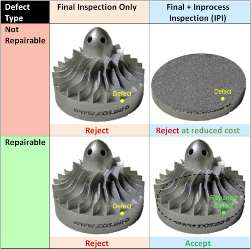
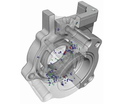
Today it appears that Blanther’s invention—3D topographical maps—could play a role in AM’s evolution. Flightware Inc., a technology consulting company based out of Guilford, Connecticut, is under contract with NASA to develop a real time, in-situ topographical inspection system for metal powder-bed processes. Flightware’s method, called layer topographic mapping (LTM) aims to detect melt layer flaws as soon as the layer is complete and without the need for human interpretation. Rather than performing a CT scan after the entire build sequence is finished, Flightware’s system accomplishes the same effect during the build. Flaws are detected by topographically mapping each layer and comparing that data to nominal solidification conditions. This inspection is performed simultaneous to the powder recoat operation, so the build time remains unchanged.
Flightware president David Maass says that LTM represents a marked difference from current in-situ AM inspection systems such as meltpool monitoring. As we have recently covered, in-situ meltpool monitoring allows us to peer inside metal powder beds at a microscopic level during a laser powder-bed fusion process. Using this technique, we can witness how the laser melts and shapes the powder both at the surface and below the melt pool. Yet, while meltpool monitoring can be used to quantify the formation of defects, Maass points out that it doesn’t allow for direct measurement of the formed metal layer quality. While melt pool monitoring offers strong correlation to defects, melt pool monitoring nevertheless measures the process, not the end product. It also does not allow for automated accept/reject criteria to effectively make decisions from the data provided.
“The basic premise of what we’re doing is the fact that topography info has value, and there is information embedded in topography that we can exploit for our purposes.”
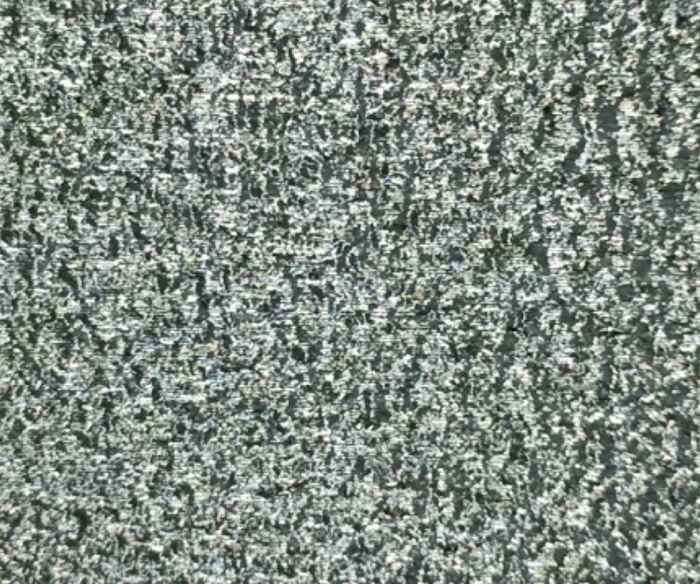
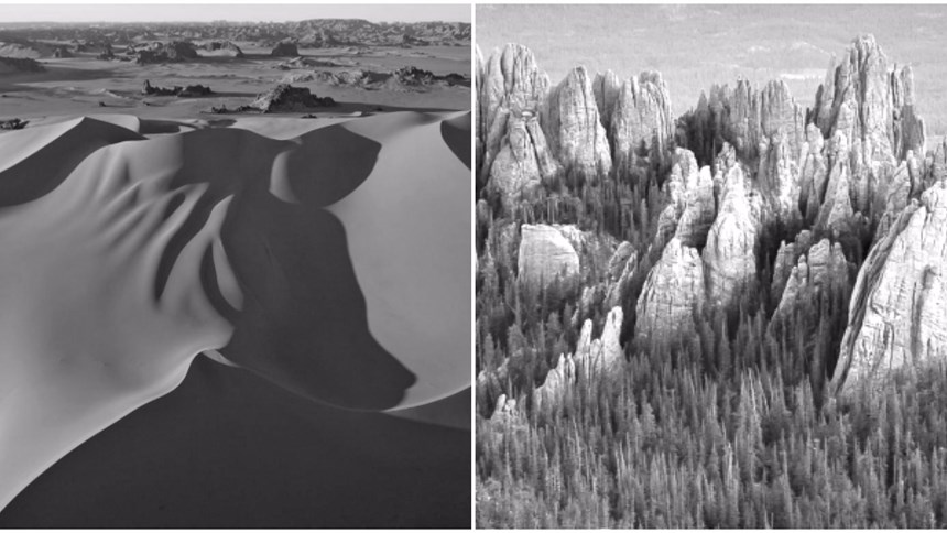
Conversely, LTM processes detect melt layer flaws upon creation by scanning each layer’s topography. Consider the Earth’s terrain as a comparison: Clear topographical distinctions easily can be made between, say, the Sahara Desert and a volcano on the Hawaiian Islands. Similarly, LTM processes employ a commercial laser profilometer working inside the build chamber to pinpoint the distinctive topographical characteristics of a newly formed metal layer at a submicron resolution. Flightware’s software then processes the scanned topography data to detect subtle differences between a “good” quality melt and “flawed” melt qualities such as porosity, unused powder, and curled layers. The software algorithms are tuned to detect, record and display those flawed regions as they’re created, which gives an operator the chance to reject the flawed part early in the build process. One day, says Maass, perhaps the technology will even be used to allow the machine to automatically repair the flaw before additional layers are added.
As phase one of the Flightware’s contract with NASA wraps up, Maass is hoping to procure a second phase to tackle existing challenges with LTM. The algorithms are still being tweaked to reduce the occurrence of false positives. And while profilometers used during phase one were able to scan 15-mm sections of each layer, practical use of LTM would call for a way to scan the entire powder bed. Flightware is collaborating with the Edison Welding Institute using its L-PBF test bed to fabricate and inspect test coupons. (Flightware is also interested in partnering with a 3D printer company during phase two of its research that can design a sensor system for use as a commercial option.) Additionally, the datasets created by the profilometer scans—even the small scans being performed now—contain millions of data points that can resolve layer height to within two-tenths of a micron. It’s an extremely dense and detailed look at the layer topography, which results in predictably large datasets that require parallel processing capabilities.
Still, LTM has the potential to hasten metal AM’s evolution—especially for aerospace and NASA, which has a vested interest in elevating the sophistication of its low-volume, high-value supply chain. While Flightware is still developing this technology, Maass says that a functional LTM system promises to save time, prevent waste, reduce unit costs, and increase productivity. “The basic premise of what we’re doing is the fact that topography info has value,” he says, “and there is information embedded in topography that we can exploit for our purposes.”
Related Content
This Year I Have Seen a Lot of AM for the Military — What Is Going On?
Audience members have similar questions. What is the Department of Defense’s interest in making hardware via 3D printing over conventional methods? Here are three manufacturing concerns that are particular to the military.
Read MoreVideo: 5" Diameter Navy Artillery Rounds Made Through Robot Directed Energy Deposition (DED) Instead of Forging
Big Metal Additive conceives additive manufacturing production factory making hundreds of Navy projectile housings per day.
Read MoreHow Norsk Titanium Is Scaling Up AM Production — and Employment — in New York State
New opportunities for part production via the company’s forging-like additive process are coming from the aerospace industry as well as a different sector, the semiconductor industry.
Read MoreAdditive Manufacturing Is Subtractive, Too: How CNC Machining Integrates With AM (Includes Video)
For Keselowski Advanced Manufacturing, succeeding with laser powder bed fusion as a production process means developing a machine shop that is responsive to, and moves at the pacing of, metal 3D printing.
Read MoreRead Next
The Value of Metal and Powder Simulation
Two videos from Lawrence Livermore National Laboratories show how SLM works at the powder level.
Read MoreValidating and Qualifying
X-ray technology can validate the internal geometry of additively-manufactured parts in 3D without destroying the part.
Read MorePostprocessing Steps and Costs for Metal 3D Printing
When your metal part is done 3D printing, you just pull it out of the machine and start using it, right? Not exactly.
Read More

